




India Domestic Chip Mandate for Smart Meters, Aiming to Design Chips Domestically by 2030
| General Studies Paper II: Government Policies and Interventions |
Why in News?
Recently, India mandated the use of locally designed and fabricated semiconductor chips in smart electricity meters by mid-2028, driving a broader strategic transition toward full technological self-reliance.
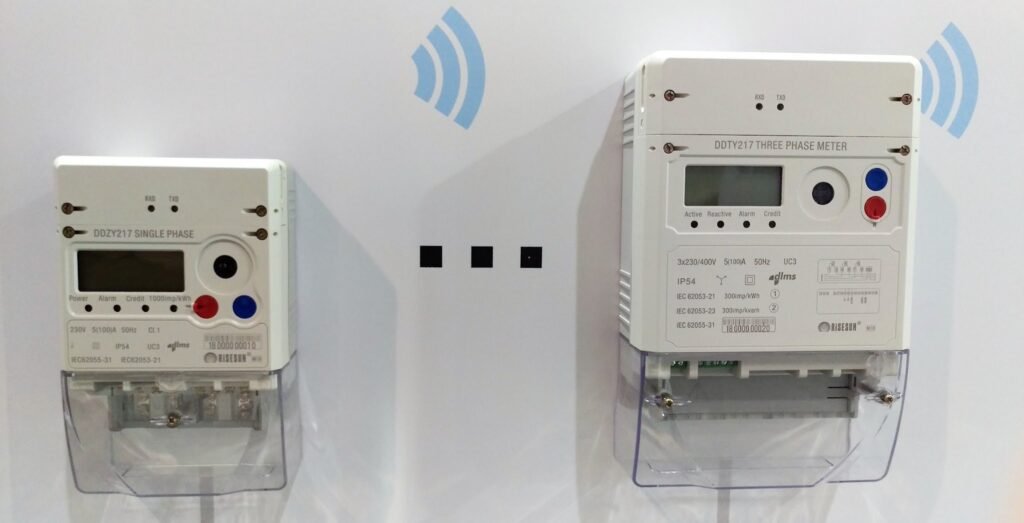
Highlights of India’s Domestic Chip Mandate for Smart Meters
- Proposal: On 24 September 2026, Power Secretary stated that India plans to mandate “design-in-India” chips for smart meters by mid-2028, with fabrication in India also envisaged around the same timeline.
- The proposed approach follows a logical design → validation → commercialisation → fabrication sequence.
- Rationale:
- Smart-meter chips are currently entirely imported, according to the Power Secretary.
- The reported chip cost is approximately US$8–10 per meter, making semiconductor localisation relevant potentially to the input-cost structure of smart-meter manufacturing.
- The government expects public procurement to provide an assured market for Indian-designed chips.
- This creates a demand-side industrial policy mechanism, potentially helping domestic developers.
- Indigenous chip design can provide greater control over hardware architecture, firmware, security features and trusted supply chains, reducing dependence on external technology providers.
- Smart-meter deployment is already being undertaken at enormous scale through the Revamped Distribution Sector Scheme (RDSS).
- As of March 2026, 20.33 crore smart meters had been sanctioned under RDSS, while 5.97 crore had been installed nationally across schemes.
- The mandate fits into India’s broader Atmanirbhar Bharat semiconductor strategy.
- As of March 2026, 20.33 crore smart meters had been sanctioned under RDSS, while 5.97 crore had been installed nationally across schemes.
- Smart-meter chips are currently entirely imported, according to the Power Secretary.
What Is a Smart Meter?
- About: A smart meter is a digitally enabled electricity meter capable of measuring consumption and communicating information remotely.
- Unlike conventional meters requiring physical reading, smart-meter systems support automated data collection, remote communication and digital energy accounting.
- Semiconductor Functions: The semiconductor architecture typically performs functions such as measurement, computation, communication, memory, power management and security.
- The chip therefore becomes the technological core connecting the physical measurement of electricity with the digital Advanced Metering Infrastructure (AMI).
- AMI consists broadly of smart meters, communication networks, Head-End Systems (HES) and Meter Data Management (MDM).
- CEA maintains technical specifications and guidelines for end-to-end communication between smart meters, HES and MDM.
- The chip therefore becomes the technological core connecting the physical measurement of electricity with the digital Advanced Metering Infrastructure (AMI).
- Two-Way Communication: A major distinction is bidirectional communication.
- Utilities can receive consumption information remotely while authorised commands or configuration information can move towards meters.
- This enables remote monitoring, prepaid functionality, faster fault identification and operational management.
- Loss Reduction: Smart meters provide actual consumption data, reducing dependence on estimated readings and manual meter-reading errors.
- They can also support identification of abnormal consumption patterns and electricity theft.
- Under RDSS, AI/ML-based analysis of smart-meter data is envisaged for theft detection and energy accounting.
- Prepaid Electricity: RDSS strongly promotes prepaid smart metering. In December 2025, the government stated that 97% of the 20.33 crore smart meters sanctioned under RDSS were intended to be in prepaid mode.
- Prepaid functionality can improve collection efficiency and help DISCOMs manage revenue risks.
- Time-of-Day Tariff: Smart meters also enable more sophisticated tariff systems.
- Under the 2023 amendment to Electricity (Rights of Consumers) Rules, Time-of-Day tariffs provide lower tariffs during designated solar hours and higher tariffs during peak periods.
- Grid Modernisation: Aggregated smart-meter data can improve load forecasting and power procurement, helping utilities manage demand and reduce supply costs.
- Challenges:
- Smart meters transform electricity meters from relatively isolated measuring devices into connected digital endpoints.
- Their large-scale deployment therefore expands the cyber-attack surface of the electricity-distribution network.
- A compromised or poorly secured chip, firmware layer or communication interface can create vulnerabilities that persist throughout the device lifecycle.
- Electricity systems are fundamental to economic and national functioning. Cyber disruption affecting large numbers of connected meters could potentially affect billing, consumer services, operational visibility and distribution management.
- The Central Electricity Authority issued its Cyber Security in Power Sector Guidelines in 2021 and maintains a dedicated regulatory framework for cybersecurity.
- AMISP providers are required to prepare a “Privacy by Design” document describing the processes and technologies used to protect and process smart-meter information.
- The RDSS framework specifies that only Government of India “MeghRaj” cloud services or MeitY-empanelled cloud services should be used for the relevant AMI environment.
India’s Semiconductor Ecosystem
- Policy: India launched the Semicon India Programme with a ₹76,000-crore outlay to establish a semiconductor and display ecosystem covering fabs, packaging, testing, design and related infrastructure.
- The India Semiconductor Mission (ISM) functions as the institutional framework for this strategy.
- Chip Design Pipeline: India’s foundational design landscape is centered around the Digital India RISC-V (DIR-V) Programme, which produces open-source architectures like SHAKTI and AJIT to reduce reliance on foreign-licensed architectures.
- State of Intellectual Property (IP) Creation: The Center for Development of Advanced Computing (C-DAC) developed DHRUV64, alongside commercial launches such as the ISC VegaSOM.
- This represents a shift from “designing for global companies” toward owning local semiconductor patents and intellectual property.
- Institutional Access Expansion: Under the Chips to Startup (C2S) Programme, Electronic Design Automation (EDA) tools have been expanded to over 400 engineering institutions and 105 startups, allowing tier-II and tier-III city students to design more than 250 test chips.
- Commercial Fabrication Facilities: Under the initial phases of the ISM, 12 manufacturing projects have been approved across six states, with major facilities established in Dholera, Gujarat (Tata Electronics in partnership with PSMC).
- OSAT and ATMP Capabilities: Recognizing that fabrication takes longer to scale up, India prioritizes Outsourced Semiconductor Assembly and Test (OSAT) and Assembly, Testing, Marking, and Packaging (ATMP) units.
- Five commercial packaging units have already reached operational production stages.
- Specialized Foundries: Current operational roadmaps emphasize Compound Semiconductors (e.g., Silicon Carbide and Gallium Nitride) and Radio Frequency (RF) chips.
- These technologies require lower capital outlays compared to advanced logic sub-7nm nodes, but are critical for Electric Vehicles (EVs), 5G networks, and strategic defense equipment.
- Critical Material Upstream Vulnerabilities: India remains heavily dependent on foreign imports for basic raw materials, including high-purity silicon wafers, electronic-grade specialty chemicals, ultrapure gases, and photoresists.
- Advanced photolithography equipment (such as ASML’s EUV/DUV machines) cannot be manufactured domestically.
- Ancillary MSME Integration: To stabilize local supply chains, the domestic strategy links semiconductor clusters with precision-manufacturing MSMEs. These small-scale manufacturers provide high-tolerance industrial packaging, tooling, and electronic components.
- Fiscal Architecture: The regulatory framework has transitioned through an expansive multi-tiered funding approach:
| Policy Framework | Fiscal Outlay | Primary Focus Areas |
| Semicon India 1.0 (2021) | ₹76,000 Crore | Initial setup of silicon fabs, display foundries, and primitive packaging units. |
| Semicon India 2.0 (2026) | ₹1,27,500 Crore | Deepening value chains: equipment, specialty materials, R&D, and local IP creation. |
| Electronics Components Scheme (ECMS) | ₹40,000 Crore | Funding upstream passives, PCB assembly, and basic hardware components. |
- Design-Linked Incentive (DLI) Scheme: This program offers financial subsidies up to 50% of eligible expenditure along with deployment-linked incentives.
- Under the Design Linked Incentive (DLI) Scheme, 24 semiconductor design projects have received support, while more than 1 lakh engineers from 500 organisations have received access to advanced chip-design tools.
- Standardized Fiscal Support Parity: To maintain global competitiveness, the central government offers uniform financial support of 50% of the project cost across all technology nodes for setting up fabrication units and packaging plants.
- Institutional Roadmap:
- NITI Aayog Vision 2035: The official 10-year strategy aims to scale India’s domestic semiconductor value chain to $120–150 Billion by 2035. This objective is supported by an estimated cross-sector investment target of $135–180 billion.
- Human Capital Milestone: By integrating semiconductor process engineering curriculums across universities, India achieved its target of training 85,000 specialized semiconductor engineers within a four-year period.
- Geopolitical and Strategic Alignment: The long-term roadmap aligns with international partnerships—such as the US-India iCET initiative, the India-Japan Semiconductor Supply Chain Partnership, and EU agreements. These bilateral deals focus on securing technological access, co-developing advanced packaging, and maintaining global supply chain resilience.
- Talent Pipeline: The government reported that approximately 85,000 semiconductor engineers had been developed against the original ten-year target in four years.
- Global Supply-Chain Integration: India is simultaneously pursuing international semiconductor partnerships, including cooperation with the United States, Japan, European Union, Singapore and Netherlands. India also joined Pax Silica in 2026.
Frequently Asked Questions (FAQs):
1. When will India mandate domestic chips for smart meters?
India plans to mandate India-designed smart-meter chips by mid-2028, potentially including chips fabricated domestically.
2. Why is India planning domestic chips for smart meters?
The move aims to strengthen cybersecurity, reduce imported-chip dependence, and develop domestic semiconductor capabilities.
3. What is the smart meter chip mandate from 2028?
From mid-2028, smart meters are expected to use domestically designed chips, with domestic fabrication also envisaged.
4. Will smart meters use India-designed chips?
Yes. The government intends smart meters to use India-designed chips, following successful testing and validation by developers.
5. How will domestic chips improve smart meter cybersecurity?
Domestic design can provide greater control over chip architecture, security features and supply chains, reducing exposure to externally controlled technologies.
Disclaimer: Information in this article is based on official announcements and public records. Details may evolve over time.